Command Palette
Search for a command to run...
Google Reveals Its Secret Weapon TPU, AlphaChip Appears in Nature! In-depth Analysis of the Development of AI Design Chips
In 2020, Google published a landmark preprint paper "Chip Placement with Deep Reinforcement Learning", showing the world for the first time its chip layout designed using a new reinforcement learning method.This innovation enabled Google to introduce AI into the chip design of TPU, achieving chip layout that surpasses human designers.
By 2022, Google further open-sourced the algorithm code described in the paper, allowing researchers around the world to use this resource to pre-train chip blocks.
Today, this AI-driven learning method has been tested by multiple generations of products, including TPU v5e, TPU v5p, and Trillium, and has achieved remarkable results within Google. Even more impressive is that the Google DeepMind team recently published an appendix to the method in Nature, which elaborated in more detail on its profound impact on the field of chip design. At the same time,Google also opened a pre-trained checkpoint based on 20 TPU modules, shared the model weights, and named it AlphaChip.
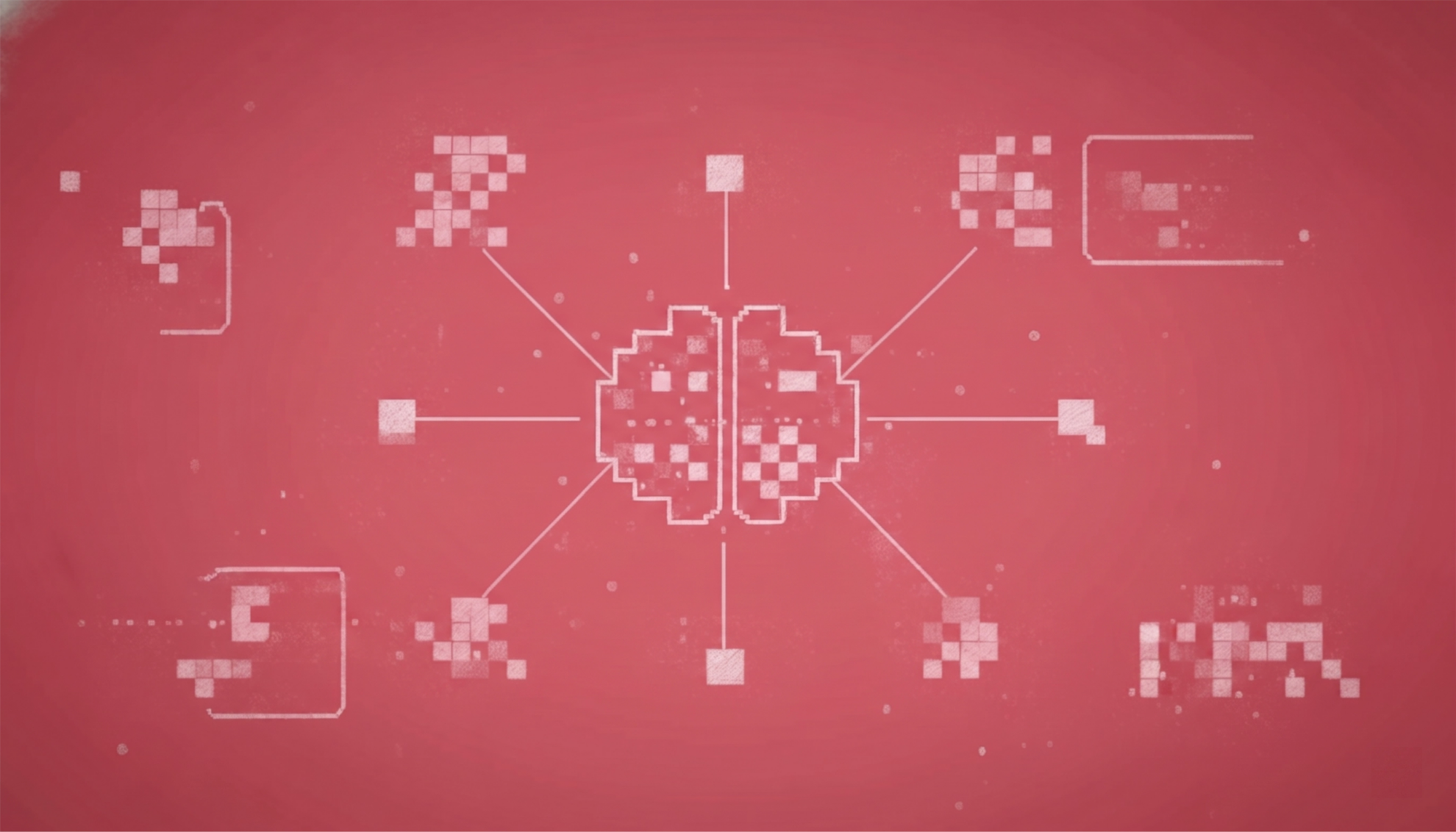
The advent of AlphaChip not only indicates that the application of AI in the field of chip design will become more extensive, but also marks that we are moving towards a new era of "chip designing chips".
AlphaChip: How Google DeepMind is using AI to revolutionize chip design
As the pinnacle of Google DeepMind, AlphaChip is capturing the attention of the global technology community with its revolutionary progress in chip design.
Chip design is a field at the pinnacle of modern technology, and its complexity lies in cleverly connecting countless precision components through extremely fine wires. As one of the first reinforcement learning technologies applied to solve real-world engineering problems, AlphaChip can complete chip layout design comparable to or better than humans in just a few hours, without the need for weeks or months of manual labor. This epoch-making progress has opened the door to our imagination beyond traditional limits.
So how exactly does AlphaChip accomplish this feat?
The secret of AlphaChip is the reinforcement learning principle it uses, which treats chip layout design as a game. Starting from a blank grid, AlphaChip gradually places each circuit component until all are in place. Then, the system will give corresponding rewards based on the quality of the layout.
More importantly, Google innovatively proposed an edge-based graph neural network.This enables AlphaChip to learn the relationships between chip components and apply them to the design of the entire chip, thereby achieving self-transcendence in each design. Similar to AlphaGo, AlphaChip can learn through "games" and master the art of designing excellent chip layouts.
In the specific process of designing the TPU layout, AlphaChip first pre-trains on various modules of previous generations of chips, including on-chip and inter-chip network modules, memory controllers, and data transfer buffers. This pre-training phase provides AlphaChip with rich experience. Subsequently, Google uses AlphaChip to generate high-quality layouts for current TPU modules.
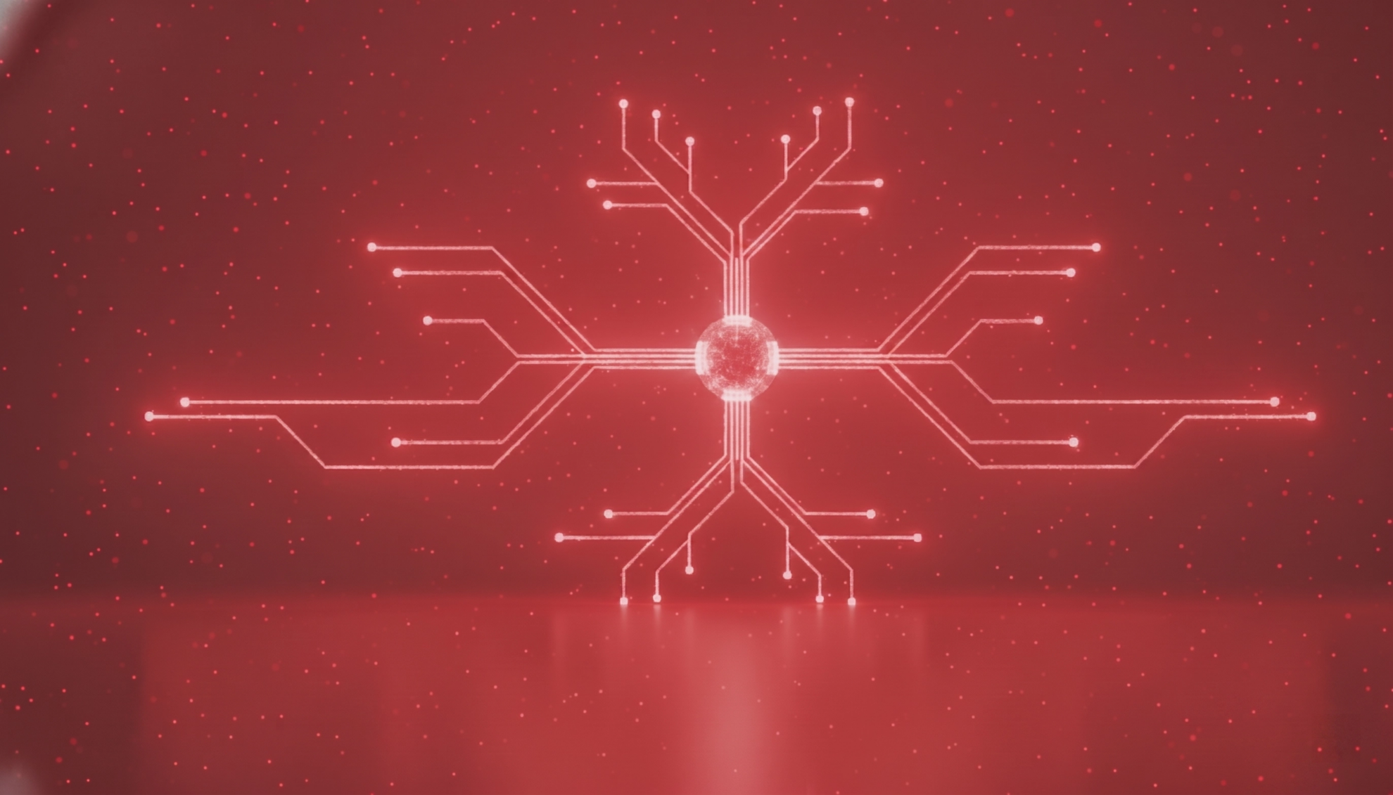
Unlike traditional methods, AlphaChip continuously optimizes itself by solving more chip layout tasks, just as human experts continuously improve their skills through practice. As DeepMind co-founder and CEO Demis Hassabis said,Google has built a powerful feedback loop around AlphaChip:
* First, train an advanced chip design model (AlphaChip)
* Second, use AlphaChip to design better AI chips
* Then, use these AI chips to train better models
* Finally, use these models to design better chips
This repetitive process enables the simultaneous upgrade of models and AI chips. Demis Hassabis said, "This is part of the reason why Google's TPU stack performs so well."
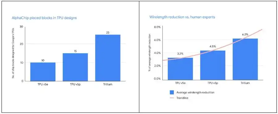
Compared to human experts, AlphaChip not only places more modules, but also significantly reduces the wiring length.With each new generation of TPU, AlphaChip designs a better chip layout, providing a more complete overall floor plan, thereby shortening the design cycle and improving chip performance.
Google TPU's 10-year journey: from ASIC persistence to AI design innovation
As an explorer and pioneer in the TPU field, Google's development history in this technology line not only relies on its keen insight, but also demonstrates its extraordinary courage.
As we all know, in the 1980s,ASIC (Application Specific Integrated Circuit) is characterized by its high cost-effectiveness, strong processing power and high speed.However, the functions of ASIC are determined by customized mask tools, which means that customers need to pay expensive upfront non-recurring engineering (NRE) fees.
at this time,FPGA (Field Programmable Gate Array) has the advantages of lowering upfront costs and reducing the risks of customizing digital logic.It has come into the public eye, and although it does not surpass all other models in terms of performance, it is unique in the market.
At the time, the industry generally predicted that Moore's Law would push FPGA performance beyond the needs of ASICs. However, it turns out that FPGA, as a programmable "universal chip", performs well in exploratory and small-batch products and can achieve better speed, power consumption or cost indicators than GPUs, but it still cannot escape the law that "universality and optimality cannot be achieved at the same time." Once FPGA paves the way for a dedicated architecture, it will give way to more professional ASICs.
After entering the 21st century, the AI technology boom has been rising. Machine learning and deep learning algorithms have continued to iterate. The industry's demand for high-performance, low-power dedicated AI computing chips has increased. CPUs and GPUs are unable to cope with many complex tasks. Against this background, Google made a bold decision in 2013.ASICs were chosen to build TPU infrastructure and develop around TensorFlow and JAX.
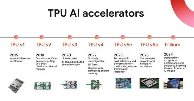
It is worth noting that self-developed ASIC is a long process with high investment, high threshold and great risk. Once the wrong direction is chosen, it may lead to huge economic losses. However, in order to explore more cost-effective and energy-saving machine learning solutions, Google immediately started developing TPUv1 in 2013 after making a breakthrough in image recognition through deep learning in 2012, and announced the internal launch of the first generation of TPU chip (TPU v1) in 2015.This marks the birth of the world's first accelerator designed specifically for AI.
Fortunately, TPU soon had a striking demonstration opportunity - in March 2016, AlphaGo Lee successfully defeated the world Go champion Lee Sedol. As the second-generation version of the AlphaGo series, it runs on Google Cloud and consumes 50 TPUs for calculations.
However, TPU did not immediately achieve large-scale successful applications in the industry. It was not until the AlphaChip chip layout method was proposed that TPU truly entered a new stage of development.
In 2020, Google demonstrated the capabilities of AlphaChip in a preprint paper titled “Chip Placement with Deep Reinforcement Learning”.It is able to learn from past experience and continuously improve by designing a neural architecture that can accurately predict rewards on a variety of netlists and their layouts, generating rich feature embeddings for the input netlist.
AlphaChip regards the conditions for performance optimization as the conditions for winning the game, and uses reinforcement learning to train an intelligent agent to maximize the cumulative reward and continuously optimize the chip layout capabilities. They started 10,000 games, allowing AI to practice layout and routing on 10,000 chips and collect data, while continuously learning and optimizing.
Ultimately, they found that AI performed as well or as well as manual layout in terms of area, power, and wire length as human engineers, while meeting design criteria in significantly less time.AlphaChip can generate layouts on modern accelerator netlists that rival or exceed manual performance in less than 6 hours.Under the same conditions, existing human experts may need several weeks to complete the same task.
With the help of AlphaChip, Google's reliance on TPU is increasing. December 2023Google has launched three different versions of the multimodal general-purpose large model Gemini, which makes extensive use of Cloud TPU v5p chips for training. May 2024Google has released the sixth-generation TPU chip Trillium, which can be expanded into a cluster of up to 256 TPUs in a single high-bandwidth, low-latency Pod. Compared with previous generations, Trillium is more powerful in adapting model training.
At the same time, TPU chips have gradually moved beyond Google and gained wider market recognition. July 30, 2024Apple claimed in a research paper that it selected two Google Tensor Processing Unit (TPU) cloud clusters when training the artificial intelligence model AFM in the Apple Intelligence ecosystem. Other data shows that more than 60% of generative AI startups and nearly 90% of generative AI unicorns are using Google Cloud's AI infrastructure and Cloud TPU services.
All signs indicate that after a decade of hard work, TPU has stepped out of its incubation period and is beginning to contribute to Google's AI era with its excellent hardware performance.The "AI designing AI chip" path contained in AlphaChip has also opened up new horizons in the field of chip design.
AI revolutionizes chip design: From Google AlphaChip to the exploration of full process automation
While AlphaChip is unique in the field of AI-designed chips, it is not alone. The tentacles of AI technology have been widely extended to many key links such as chip verification and testing.
The core task of chip design is to optimize the power consumption, performance and area of the chip. These three key indicators are collectively referred to as PPA. This challenge is also called design space exploration. Traditionally, this task is completed by EDA tools, but in order to achieve optimal performance, chip engineers must constantly adjust manually, and then hand it over to EDA tools for optimization again, and so on. This process is like placing furniture at home, constantly trying to maximize space utilization and optimize traffic flow, but each adjustment is equivalent to moving the furniture out and rearranging it, which is extremely time-consuming and labor-intensive.
In order to solve this problem,Synopsys launched DSO.ai in 2020.This is the industry's first chip design solution that integrates AI and EDA. DSO.ai uses reinforcement learning technology to automatically search the design space through AI to find the best balance point without human intervention. This tool has been used by many chip giants.
For example, Microsoft reduced the power consumption of chip modules by 10%-15% after using DSO.ai, while maintaining the same performance; STMicroelectronics increased PPA exploration efficiency by more than 3 times; and memory chip giant SK Hynix reduced chip area by 5%. According to Synopsys data, DSO.ai has successfully assisted more than 300 commercial tape-outs, indicating that AI plays an important role in real chip design and production.
In terms of AI-assisted chip verification, a technical report released by Synopsys also pointed out that the verification process takes up to 70% of the entire chip development cycle. The cost of a chip tape-out is as high as hundreds of millions of dollars, and the complexity of modern chips continues to increase, making verification more difficult.Synopsys has launched the VSO.ai tool.Use AI to optimize the verification space and accelerate the convergence of coverage.
VSO.ai can infer different types of coverage, complementing traditional code coverage, and AI can also learn from verification experience and continuously optimize coverage targets. In addition, Synopsys has also launched the TSO.ai tool, which can help chip developers screen out defective chips manufactured by foundries.
The deep involvement of AI in chip design has triggered a bold idea: Can we use AI to design a complete chip? In fact, NVIDIA has already tried this. By using deep reinforcement learning agents to design circuits,Nearly 13,000 circuits in Nvidia's H100 were designed by AI. The Institute of Computing Technology of the Chinese Academy of Sciences also used AI to generate a RISC-V processor chip called "Enlightenment No. 1" in 5 hours.With 4 million logic gates, its performance is comparable to the Intel 80486.
Overall, AI's ability to design complete chips is still limited, but this is undoubtedly an important opportunity for future chip development. With the continuous advancement of technology, AI's potential in the field of chip design will be further explored and utilized, and will ultimately change the entire chip design process.